Atomically thin materials instead of silicon as the basis for transistors
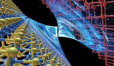
The use of atomically thin materials instead of silicon as the basis for new transistors is exciting but connecting those ‘2D’ materials to other conventional electronic components has proved difficult. Now researchers at MIT, the University of California at Berkeley, the Taiwan Semiconductor Manufacturing Company, and elsewhere have found a new way of making those electrical connections, which could help to unleash the potential of 2D materials and further the miniaturisation of components—possibly enough to extend Moore’s Law, at least for the near future. The 2D materials or sheets, just a few atoms thick, meet all the requirements for enabling miniaturisation, potentially reducing by several times a key parameter called the channel length, from around 5 to 10 nanometres in current cutting-edge chips to a sub-nanometer scale. At the interface between the semimetal (bismuth) and the 2D semiconductor (MoS2), there is no energy barrier for the electron to go t